
Features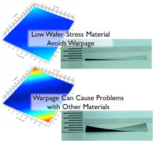
Overview
PDM-5022 is a dielectric material with an exceptionally high breakdown strength. It is also NMP-free, which simplifies regulatory compliance.
Dielectric materials also need to endure the stresses associated with device packaging. The heat generated at the time of component packaging can cause substrate warpage. This then causes stress on the component joints, decreasing packaging and product reliability.
PDM-5022 has been utilized to minimize stress caused by polymer coatings. Typical materials like polyimide have a high modulus and a high cure temperature, which causes the material to shrink. This is counter-productive to low wafer stress.
By employing a non-shrinking, low cure temperature (180 ̊C) mechanism in combination with low modulus (1.2 GPa), PDM-5022 was designed to reduce wafer curvature (15 μm; 7 MPa stress) and reduce overall package stress.
These attributes make PDM-5022 a suitable dielectric for advanced packaging applications that require low stress and high thermal stability.
Properties
| Tensile Strength | 27 MPa |
| Modulus | 1.2 GPa |
| Elongation | 24% |
| Glass Transition Temperature (Tg) | 280 ̊C |
| Coefficient of Thermal Expansion (CTE) | 212 ppm |
| 5% and 95% Weight Loss | 286 ̊C and 514 ̊C |
| Dielectric Constant | 2.7 at 1 MHz |
| Dielectric Breakdown Strength | 420kV/mm |
| Moisture Uptake | 0.1% |
| Wafer Warpage | 15.7 µm |
| Internal Stress | 7 MPa |
| Chemical Resistance | Good |
| Adhesion to Metals | Excellent |
Promerus is a technology-driven organization providing advanced material solutions for the next generation of applications. These materials are based on high-purity cyclic olefin polymers that provide outstanding electrical, mechanical, optical and thermal properties. For more information, fill out the form below to explore our full list of materials and applications.